Hi, welcome back to our Hardcaml MIPS project! Before we dive into the actual project, I wanted to provide a bit of background on how hardware and computers work, and why I hope Hardcaml might be a good tool for hardware design. This is part 2 of this intro: in part 1 we covered how computers and CPUS actually work.
Hardware Design 101
Assuming my ramblings from the previous post make sense, you should now have a basic understanding of what CPUs do, and how basic hardware works. Now, we need to connect the two.
Often, we'll design hardware in terms of "modules", which are circuits that represent some behavior. For example:
- A multiplexor takes several inputs and a "selector" value, and outputs one of the inputs as indicated by that "selector". You can think of a multiplexor as a ternary, but with an arbitrary number of inputs.
- A memory block could be composed of registers, and take inputs that control reads/writes. For example, it might take an input indicating which part of memory we want to read, and output the value at that area in memory.
- An ALU (arithmetic logic unit) could take 2 "value" inputs, and an "operation ID" input. Depending on the operation ID, it would output the sum/product/shift of the 2 inputs.
- A sign extender could convert a 16-bit value to a 32-bit value by repeating the 16-bit input's most significant bit for the 16 new bits. These notes are a good resource for understanding how signed (positive/negative) values are encoded in binary.
And so on. Very frequently, hardware designers will create small modules that abstract away some operation, and use those modules in other, larger modules.
By the way, it's very, very important to remember that hardware is NOT software. In the software world, we have a stream of expressions (which all somehow map to CPU instructions), and we can jump around our program depending on various conditions. In hardware, you can't "call" a circuit: circuits are physical clumps of wires and logic gates that actually, physically exist. So while we can model circuits as stateful and non-stateful functions that convert inputs to outputs, we need to remember that all our circuits are always processing electrons and producing output (in parallel!).
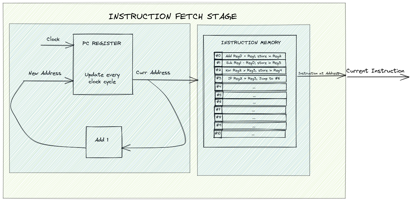
Let's go back to our 5-stage MIPS CPU design, and discuss how we can implement the Instruction Fetch stage in terms of modules/circuits.
- Fetch. Here, we figure out where we are in the program and fetch the next instruction from memory.
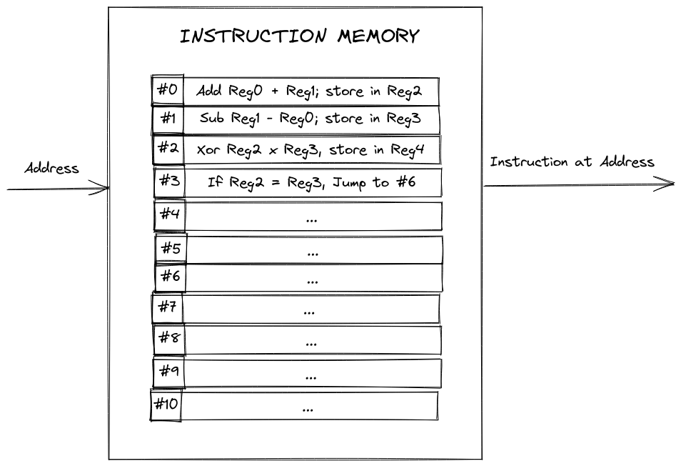
To keep things simple, let's assume that we have a hardcoded block of memory that represents the instructions we're executing. Remember that each MIPS instruction is 32 bits, so we can think of this block as a 32-wide grid of registers, where each row is an instruction, and every row number is the address of this instruction. We'll wrap this grid into a module/circuit called instruction memory. This circuit will take an input representing the address of the instruction we want to fetch, and output the actual instruction at the given address.

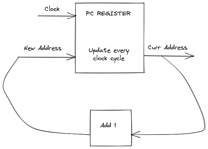
The other thing we'll need is to keep track of where we are in the program. We'll want to use a register (called the PC, or Program Counter register), which stores our current address and emits it as an output. We'll also take a new address as an input, and update our stored address to the new one every clock cycle (since we fetch one instruction every cycle). We don't want to worry about jumps/branches for now, so the new address will just be the curr_address + 1.

Putting it all together, we've designed the core instruction fetch stage of our CPU. Yay!

Verilog, and why I don't like it
Historically, hardware designers had to manually arrange logic gates and wires. Luckily, tools were developed that allow us to describe our hardware in a RTL (Register Transfer Layer) language, which represents how data signals flow through circuits. Then, software synthesises that RTL into a netlist, which represents the actual layout of gates and wires.
The most used RTL languages are Verilog and VHDL. Here, we'll be talking about Verilog because that's what I learned in class. For an example, let's design the PC Register from the previous section in Verilog:
module pc_reg (
    input clk,
    input [31:0] pc_next,
    output reg [31:0] pc
);

initial pc = 0;

always @(posedge clk) begin
    pc <= pc_next;
end

endmodule
Simple enough: on every positive clock edge (i.e. once per cycle), we replace the stored address with a new one. We constantly emit the current address as output, and our inputs are the next address and the clock. It's concise, clear, and simple: almost as if Verilog was originally designed to serve as documentation and describe simulations. Oh wait...
Originally, Verilog was only intended to describe and allow simulation; the automated synthesis of subsets of the language to physically realizable structures (gates etc.) was developed after the language had achieved widespread usage.
And that's the issue. Verilog is great at what it's supposed to do: describing circuits and simulating events. But when we start trying to write anything larger than a simple circuit, we start running into issues (at least in Vivado, the dominant IDE for hardware design):
- The synthesis process doesn't throw error in cases where you would expect it to:
- You can have multiple modules / circuits outputting to the same wire. Understandably, when this happens the simulation gets really confused and doesn't show anything meaningful. It'll still synthesize though.
- You can pass wires into a module by name, but it won't error if a wire is missing, misnamed, etc. As I mentioned in the intro post for this series, @DoperBeats and I once spent an hour debugging only to find that I mistyped a wire name.
- You can pass a 1-bit wire to a 5-bit port on a module (or any other mismatched combination). I imagine there might be genuine use cases for this, but often this means you made a typo. Explicitly extending/truncating signals is already possible by making a module to transform your input/output, so I'm not sure why this implicit conversion should be allowed.
- On the rare occasions you do get errors/warnings, they're generally cryptic and require relatively deep understanding of Verilog. Not great for beginners.
- Tooling sucks
- All the synthesis errors I complained about above could be identified through static analysis and surfaced as warnings/errors in the editor. Emphasis on could be.
- The rare errors you do get are hard for beginners to understand.
- Want to write code in a different editor like VSCode? Alright, but you'll need to manually register every new file you make in Vivado. Oh, and there's no syntax error highlighting in VSCode's Verilog extensions either.
- Don't want to use Vivado (or can't because of export controls)? The alternatives are even worse.
- And the worst by far: Vivado doesn't really have a dark mode 😱
- Testing is clunky
- Tests also have to be Verilog modules, whereas usually in software it's preferable to use functions/methods for test cases.
- Partially as a consequence of the previous point, testing requires a lot of boilerplate.
- There isn't really an ecosystem for things like continuous integration. For that matter, many testing innovations from the software world (like mocks/stubs) don't seem to carry over well to hardware.
- A lot of automated testing seems to be based around printing assertions and generating waveforms in the Vivado console/waveform viewer. That's not very automatable.
- Documentation is scarce
- A significant portion of support answers on the Xilinx (makers of Vivado) forums are links to 100-page manuals, and are almost always jargon-heavy. Not a deal breaker by any means, but quite challenging for beginners.
Maybe (to be honest, probably) some of these are due to me improperly using/configuring Vivado. But I maintain that the majority of these things (especially the synthesis issues) would be baked into a proper language by default. First impressions matter, and my semester working with Verilog has left me very frustrated at the language and its ecosystem.
One thing I want to note is that I do not consider the (relatively) low level of abstraction in Verilog to be a shortcoming. Designing good hardware requires understanding of how your design comes together in terms of gates, wires, and transistors. Generally, you'll want to draw out the modules and circuits before writing up code to describe it.
Why OCaml?
The Verilog syntax is decent for documenting functionality, but in my opinion, a more powerful representation of most simple circuits would be a function that takes inputs and produces outputs. For sequential circuits that need state, we could use a function that takes inputs and the current state, and produces outputs and the new state (or encapsulates state in something that makes it clean to work with).
As someone who's been looking for an excuse to learn a proper functional programming language for a while, this realization really excited me. And when I learned about Hardcaml, it seemed perfect. OCaml is a functional programming language with an expressive static type system. Maybe that will help eliminate some of the structural errors I mentioned earlier. Hardcaml also has libraries for automated testing, where you put in the waveforms (i.e. the outputs you'd expect for various inputs and clock stages) drawn out in ASCII, and Hardcaml will simulate your circuit and compare the actual generated waveform.
There are libraries that do similar things in other languages, like Chisel for Scala and HHDL for Haskell, but I found out about Hardcaml first. Also, OCaml is more "functional" than Scala, and a bit more practical than Haskell (although eventually, I'd like to learn Haskell too).
FPGYay!
In this final, somewhat tangential section, I want to briefly explain what FPGAs are, and why they are awesome. If you're not familiar, an FPGA (Field Programmable Gate Array) is essentially reprogrammable hardware: you can configure it to represent various circuits and hardware designs as needed.
Historically, if you wanted to design hardware, you'd come up with a design and send it to a foundry. Four months and tens of thousands of dollars later, you'd get back a huge pile of chips. Let's hope you didn't make any mistakes whatsoever in your design, or that your problem hasn't suddenly changed!
The way an FPGA works is in the name: Field Programmable Gate Array. It's a huge grid of circuits called LUTs (short for lookup tables) that can represent arbitrary logic gates. The LUTs can then connected as needed to form pretty much any circuit. This means that you could purchase several FPGAs, and almost instantly reprogram them into various circuits/hardware to fix bugs, tweak your algorithm, or do something completely different. And although there is of course a cost for this abstraction, FPGA's aren't that much slower than custom-fabricated chips.
This opens up the possibility to use custom hardware (and its various performance/cost/parallelism advantages) for all sorts of problems relatively affordably.
And that's it for introductions! In the next post, we'll be diving right into our project.